- 您现在的位置:买卖IC网 > Sheet目录362799 > EVAL-AD1833AEB (Analog Devices, Inc.) 24-Bit, 192 kHz, DAC
REV. 0
AD1833A
–14–
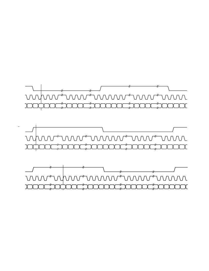
I
2
S Timing
I
2
S timing uses an
L
/RCLK to define when the data being trans-
mitted is for the left channel and when it is for the right channel.
The
L
/RCLK is low for the left channel and high for the right
channel. A bit clock running at 64 f
S
is used to clock in the data.
There is a delay of 1 bit clock from the time the
L
/RCLK signal
changes state to the first bit of data on the SDINx lines. The data
is written MSB first and is valid on the rising edge of the bit clock.
Left-Justified Timing
Left-justified (LJ) timing uses an L/
R
CLK to define when the
data being transmitted is for the left channel and when it is for
the right channel. The L/
R
CLK is high for the left channel and
low for the right channel. A bit clock running at 64 f
S
is used
LEFT CHANNEL
RIGHT CHANNEL
+1
LSB
MSB
L
/RCLK
INPUT
BCLK
INPUT
SDATA
INPUT
+2
–2
–1
MSB
+1
LSB
+2
–2
–1
MSB
Figure 6. I
2
S Timing Diagram
LEFT CHANNEL
RIGHT CHANNEL
+1
LSB
L/RCLK
INPUT
BCLK
INPUT
SDATA
INPUT
+2
–2
–1
MSB
+1
LSB
+2
–2
–1
MSB
–1
MSB
Figure 7. Left-Justified Timing Diagram
LEFT CHANNEL
RIGHT CHANNEL
+1
LSB
L/
R
CLK
INPUT
BCLK
INPUT
SDATA
INPUT
+2
–2
–1
LSB
MSB
+1
LSB
+2
–2
–1
MSB
Figure 8. Right-Justified Timing Diagram
to clock in the data. The first bit of data appears on the SDINx
lines when the L/
R
CLK toggles. The data is written MSB first
and is valid on the rising edge of the bit clock.
Right-Justified Timing
Right-justified (RJ) timing uses an L/
R
CLK to define when the
data being transmitted is for the left channel and when it is for
the right channel. The L/
R
CLK is high for the left channel and
low for the right channel. A bit clock running at 64 f
S
is used
to clock in the data. The first bit of data appears on the SDINx
8-bit clock periods (for 24-bit data) after L/
R
CLK toggles. In RJ
mode, the LSB of data is always clocked by the last bit clock
before L/
R
CLK transitions. The data is written MSB first and is
valid on the rising edge of the bit clock.
发布紧急采购,3分钟左右您将得到回复。
相关PDF资料
EVAL-AD1833EB
Multichannel 24-Bit, 192 kHz, DAC
EVAL-AD1837EB
2 ADC, 8 DAC, 96 kHz, 24-Bit Codec
EVAL-AD1837AEB
2 ADC, 8 DAC, 96 kHz, 24-Bit Codec
EVAL-AD1838AEB
2 ADC, 6 DAC, 96KHZ 24 BIT CODEC
EVAL-AD1852EB
24-Bit Stereo DAC Evaluation Board
EVAL-AD1870EB
Single-Supply 16-Bit Stereo ADC
EVAL-AD1896EB
Automotive Low-Cost Non-Volatile FPGA Family; Voltage: 1.2V; Grade: -5; Package: Lead-Free ftBGA; Pins: 256; Temperature: AUTO; LUTs (k): 8
EVAL-AD1928EBZ
2 ADC/8 DAC with PLL, 192 kHz, 24-Bit Codec
相关代理商/技术参数
EVAL-AD1833EB
制造商:AD 制造商全称:Analog Devices 功能描述:Multichannel 24-Bit, 192 kHz, DAC
EVAL-AD1835AEB
制造商:Analog Devices 功能描述:EVALUATION BOARD I.C. - Bulk
EVAL-AD1835EB
制造商:Analog Devices 功能描述:Evaluation Board For AD1835 制造商:Analog Devices 功能描述:EVALUATION BOARD I.C. - Bulk
EVAL-AD1836AEB
制造商:AD 制造商全称:Analog Devices 功能描述:Multichannel 96 kHz Codec
EVAL-AD1837AEB
制造商:Analog Devices 功能描述:EVALUATION BOARD I.C. - Bulk
EVAL-AD1837EB
制造商:Analog Devices 功能描述:EVALUATION BOARD I.C. - Bulk
EVAL-AD1838AEB
制造商:Analog Devices 功能描述:EVALUATION BOARD I.C. - Bulk
EVAL-AD1838EB
制造商:Analog Devices 功能描述:Evaluation Board For 2 ADC, 8DAC 96 KHz, 24-Bit Sigma Delta Codec 制造商:Analog Devices 功能描述:EVALUATION BOARD I.C. - Bulk